Používáte starou verzi internetového prohlížeče. Doporučujeme aktualizaci na nejnovější verzi. Některé funkce portálu nemusí být podporovány.
Pravděpodobně máte vypnutý JavaScript. Některé funkce portálu nebudou funkční.
Researchers with NenoVision are improving microscopy equipment
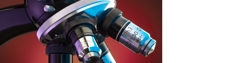
LiteScope is one of the few devices in the world that can simultaneously connect a two-dimensional image from an electron microscope and a three-dimensional image from an atomic force microscope with high precision. The product is behind the NenoVision spin-off, founded at CEITEC BUT by graduates of the Faculty of Mechanical Engineering BUT. The facilities now want to move up a class, so they have joined forces with their alma mater and scientists from the Academy of Sciences.
The two-dimensional image from the microscope is provided by an electron beam and detectors, and the three-dimensional image by a scanning probe. Both are connected by LiteScope devices, with which the Brno company NenoVision has already successfully entered the market. Now they want to add another best. They plan to turn the scanning probe into a tool that will allow you to work directly with the sample. However, the original concept, which could be described with exaggeration as "all in one box", remains. In a joint project, they will be assisted with the development of three Brno academic institutions: the Institute of Physical Engineering from FME BUT, the Institute of Materials Physics and the Institute of Scientific Instrument of the Academy of Sciences.
"Electron microscopes work with a stream of electrons in a vacuum so that the beam can reach the sample and electrons do not collide with atoms and molecules in the residual atmosphere. So we have a very clean environment where we can study the surfaces of the samples at the atomic level. Imagine, for example, a single crystal of silicon, from which chips are made, this is a very clean and orderly structure. As soon as it breaks up in the air, a "dirty" layer of adsorbed molecules from the surrounding air is formed on the originally clean surface within a millionth of a second due to the external atmosphere. Therefore, if we want to monitor what is happening at the atomic level on a clean surface, we must ensure that there is no atmosphere above it, we must work with it in the so-called ultra-high vacuum," Jiří Spousta from the Institute of Physical Engineering FME BUT explains. Inserting a sample into an electron microscope | Autor: NenoVision
In a vacuum, LiteScope already uses a scanning probe, and this is where improvements await. "We plan to use commonly available hollow optical fibres that can conduct light. Around their centre, there are micropores along the entire length of the fibre, through which we want to guide, for example, the working gas,” Spousta explains the intention. The probe will be not only a detector, but also a tool that can be used to apply light, gas or voltage to the sample, and thus work with the sample on a very small scale. What may not sound too complicated, however, becomes complicated the moment we realize what sizes we are moving in: the probes have such sharp tips that their tip consists of only tens to hundreds of atoms. "The nanostructures we research and produce are extremely small. Imagine that your hair falls on our nanostructure. The size ratio between it and a hair would be the same as if an oak with a diameter of one meter fell on your hair,” Spousta brings closer the scales that are difficult for laymen to imagine.
Improved in many ways
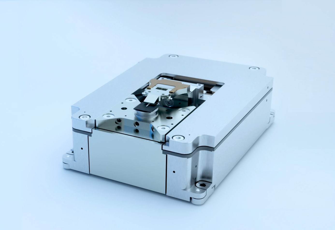
However, this is not the only improvement that NenoVision wants to contribute to the further development of microscopic techniques in collaboration with scientists. Another innovation is the device for the so-called in-situ (i.e. inside the microscope) loading, which allows to mechanically load metal samples in the vacuum chamber of the electron microscope and at the same time to observe in detail the mechanism of crack propagation that occurs on the sample. The development takes place in cooperation with the Institute of Materials Physics of the Academy of Sciences and in the future will enable a detailed study of the initial stages of the formation and propagation of fatigue cracks. Thanks to this, valuable data will be available for numerical simulations and methodologies, which are used in determining the service life of critical components, for example in the automotive or energy industries. LiteScope 2.0 device | Autor: NenoVision
The development of special calibration samples created with the help of lithographic techniques at the Institute of Instrumentation will bring further improvement to the LiteScope device. "Test specimens created in this way, based on binary and three-dimensional nanostructures, will make it possible to guarantee the correctness of dimensions both in the field of classical microscopy and in the field of the so-called correlative microscopy. This is based on the correlation of information obtained by scanning and scanning electron microscopy, where a sharp tip moves over the surface of the sample and scans. We will also deal with the tip itself and plan to use the phenomenon of quantum tunnelling in ultra-high vacuum conditions, which is a level of vacuum comparable to that on the surface of the Moon. With the help of it, we will measure the characteristics of the tips of various manufacturers so that it is possible to improve the resolution of the device and reduce the noise level," Alexandr Knápek from the Institute of Instrumentation of the Academy of Sciences adds.
The cooperation of researchers from the academic environment and the company is mutually beneficial. "With our high-tech innovative products, we are constantly striving to improve the possibilities and capabilities of microscopic techniques. It is therefore directly necessary for us to be able to connect the needs of the market and applied development. From this cooperation, we promise the emergence of new technologies and applications that push the limits of our main product LiteScope, which can significantly strengthen our position in the global market," the main researcher of the project Jan Neuman from NenoVision concludes.
Electron microscopes bring the world closer around us up to a million times, because they use electrons to image motifs, which can be accelerated and thus reduce their wavelength. This distinguishes them from their much older predecessors, optical microscopes, in which visible light is used to image a certain range of wavelengths that we are able to recognize with the eye. And because the resolution of a microscope depends on the wavelength of the radiation used, electrons "win". However, we have only used them to enlarge the image of the samples for 90 years – in Brno, the first electron microscope was built in 1951 at the Institute of Science Instrument. Today, Brno is rightly called the world's centre of electron microscopy: every third electron microscope sold in the world was made in Brno.
Published: 2021-07-14 10:36
Short URL: https://www.vut.cz/en/old/f19528/d213925