BRNO UNIVERSITY OF TECHNOLOGY
Antonínská 548/1, 601 90 Brno
Czech Republic
phone numbers list
e-mail: vut@vutbr.cz
international@vutbr.cz
http://www.vutbr.cz/en


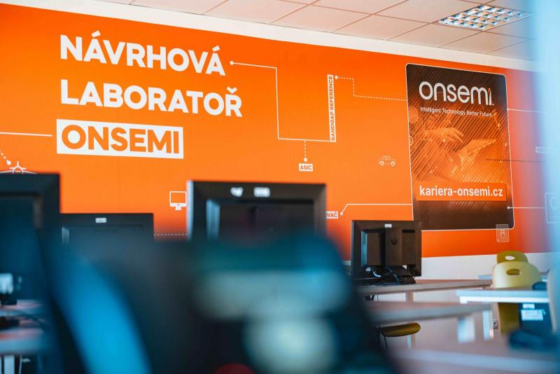
Thanks to the planned expansion of the onsemi plant in Rožnov pod Radhoštěm, there will be an increased demand for graduates in technical and electrical engineering. Within seven years, a factory for the production of silicon carbide-based chips worth CZK 46 billion will be built in Rožnov pod Radhoštěm as an extension that will allow selected modules to be produced from start to finish in one place. This will give onsemi the capability to manufacture along the entire semiconductor chain.
We discussed the challenge of this huge investment for Brno University of Technology with Jiří Háze, Head of the Department of Microelectronics at the Faculty of Electrical Engineering and Communication of Brno University of Technology (FEEC) and Vice-Chairman of the Czech National Semiconductor Cluster, and Michal Lorenc, Head of Research and Development Projects at onsemi.
What does the expansion of the onsemi plant in Rožnov pod Radhoštěm mean for the Czech Republic, Brno, and especially BUT?
Jiří Háze: It is an even greater commitment than before to educate as many technically capable graduates as possible in the field of chip design and semiconductor technology. The ways to do this were discussed at the end of June in Munich at the kick-off meeting of our new international project CHIPS of Europe. One of the steps is to innovate the curricula and introduce so-called micro-credits. At FEEC, we will open applications for the newly accredited degree programme Chip Design and Advanced Semiconductor Technology in Fall 2024. This makes it clear what we want to teach future professionals at our faculty. In turn, the mircocredits will give existing employees an opportunity to complete their education in the field and allow students to profile themselves in this direction. Graduates of such a course will receive a certificate that will help them demonstrate that they have acquired the necessary skills. The second step towards producing graduates with a technical background is to work with secondary and primary schools over a long period of time and support STEM projects. The study of technology is not just for a select few, but as our society has moved towards mass use of technology, basic technical awareness should be part of education at primary and secondary school levels.
You mention the new study programme Chip Design and Advanced Semiconductor Technology. How long does it take a student to learn how to design a chip?
Jiří Háze: Students can already learn the basics of design during their undergraduate studies, especially in this new study programme focused on these topics. The master's programme’s objective is to improve these skills and allow the students to work on more complex tasks.
For further questions, we contacted Michal Lorenc, the head of research and development projects at onsemi.
In an article in Hospodářské noviny, Aleš Cáb, Vice President and Production Director of onsemi in Rožnov, mentions that every year 70 BUT students come to onsemi for internships. I assume that FEEC students are not the only ones who find employment at onsemi. What other faculties’ graduates is onsemi interested in?
Michal Lorenc: onsemi has excellent experience with students from BUT, specifically from the Faculty of Electrical Engineering and Communication Technology, the Faculty of Information Technology, the Faculty of Mechanical Engineering and the Faculty of Chemistry. As of 2024, we have a total of 64 trainees from BUT. There are 32 in onsemi in Rožnov pod Radhoštěm and 32 in Brno.
Number of BUT students involved in onsemi internships in 2024 (as of July 2024)
|
BUT faculties |
Total number of students |
In Rožnov pod Radhoštěm |
In Brno |
|
FEEC |
41 |
16 |
25 |
|
FIT |
10 |
6 |
4 |
|
FME |
8 |
6 |
2 |
|
FCH |
5 |
4 |
1 |
Onsemi signed a memorandum of cooperation with BUT in October 2023. This is by no means a formality, but a genuine expression of interest in exploiting all opportunities for cutting-edge education, research and development in attractive areas of semiconductor technology. onsemi is a world leader in the Czech Republic (corporate centre of excellence) in the areas of semiconductor design for smart sensing (Brno) and power supply (Rožnov). In Rožnov, there are two production lines - for discrete semiconductor components (volume of over 3 billion chips per year) and semiconductor substrates (polished and epitaxial silicon and silicon carbide wafers, volume of over 3 million wafers per year). The semiconductor laboratories are also a key department with the ambition to become a global centre for the most demanding analysis. Overall, onsemi has, within the Czech Republic, a high level of complexity with a corresponding need for developers of new components as well as new technological processes, process engineers, top engineers for installation and servicing of equipment, service personnel (power and utilities provision), building and cleanroom management, IT experts, specialists in finance, purchasing, human resources and project management.
What are the most common professions in which BUT graduates are employed and how many BUT graduates do you currently employ?
Michal Lorenc: With a certain amount of perspective, we can say that graduates of FEEC and FIT find employment mainly in our design centres in Brno (development of new intelligent sensing solutions) and Rožnov (development of new power solutions), including activities in the field of testing and characterization of components and support for applications of these components. Graduates of FME and FCH have excellent prerequisites for a career in the development of new technologies and process control for the production of semiconductor materials (crystals, wafers, epitaxed wafers) and semiconductor components (chip boards). onsemi currently employs over 200 BUT graduates from top management level, through research and development, to process, production and plant maintenance engineers. BUT is therefore the most important academic partner of onsemi in the country.
From your point of view, are BUT students well prepared for practice? What else should we work on?
Michal Lorenc: We see excellent readiness for practice among students from the BUT in the long term, which stems from our joint cooperation on teaching and the organization of internships. The new study programme on chip design and semiconductor technologies will strengthen this cooperation even more. For the broad topic of semiconductor technologies, we are cooperating with BUT on the implementation of the European Chip Act - we are preparing the National Semiconductor Centre in Brno and supporting BUT's involvement in European STEM networks. The South Moravian STEM project, which aims to increase student interest in technical fields, is also important for the future. We consider it very useful to involve students in scientific projects - projects specified by onsemi or supported by onsemi, or larger programmes supported by the Czech Technology Agency.
What is the core knowledge and skills you require from BUT graduates?
Michal Lorenc: The basis is a real understanding of the principles of mathematics and physics or chemistry taught in the first years and more complex problems solved in the professional subjects of the Bachelor's and Master's degree. It is very important to be able to work effectively with information on a given professional topic. To be able to do useful professional research, to form a professional opinion, to be able to interpret it. Not to be afraid to speak and communicate. In summary – we particularly appreciate a solid technical background with a high degree of flexibility to embrace and learn new things. All of this is then positively enhanced if the technical topics are something the students really enjoy in the best sense of the word.
You also cooperate with other educational institutions. Does BUT offer onsemi something unique?
Michal Lorenc: We have had more than a quarter of a century of successful cooperation with the BUT, and BUT graduates have been instrumental in onsemi's successful growth in component design and in the development and implementation of new technologies. BUT is unique in the Czech Republic for its high level of microelectronics and radioelectronics, as well as physical engineering. Specifically for onsemi, CEITEC BUT is also crucial – both in the level of collaboration in research and development and in the opportunities for students to get real exposure to clean rooms and cutting-edge analytical and technological platforms.
Published: 2024-07-18 09:25
Short URL: https://www.vut.cz/en/old/f19528/d262085
BRNO UNIVERSITY OF TECHNOLOGY
Antonínská 548/1, 601 90 Brno
Czech Republic
phone numbers list
e-mail: vut@vutbr.cz
international@vutbr.cz
http://www.vutbr.cz/en


